Media Center
A multimedia mosaic of moments at GIST
GIST Excellence
[Press Release] Professor Kwanghee Lee"s research team develops freely bendable mesh semiconductor
- 엘리스 리
- REG_DATE : 2016.12.06
- HIT : 1316
Professor Kwanghee Lee"s research team
develops freely bendable mesh semiconductor
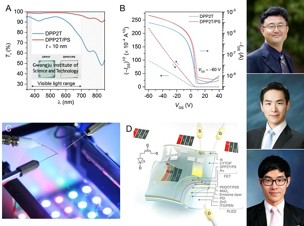
[Figure 1] (A) Optical transmittance spectrum of DPP2T thin film and DPP2T/PS thin film. The visible light transmittance of DPP2T/PS is much higher than that of pure DPP2T. (B) Transfer characteristics of DPP2T and DPP2T/PS FETs. The mobility of DPP2T/PS was increased about 4 times compared to pure DPP2T. (C) Large area transparent flexible transistor array (10cm * 10cm, 1,650 transistors) using DPP2T/PS.
(D) Transistor/organic light emitting diode junction device in which transparent flexible transistors are stacked. The stacked transistors can control the light of the organic light emitting diodes below. (Pictures from top to bottom) Professor Kwanghee Lee, Ph.D students Kilho Yu, and Byoung-wook Park.
□ A semiconductor mesh was developed that will allow for the creation of highly transparent electronic devices to bend freely as seen in movies.
□ The National Research Foundation of Korea (NRF) has announced that Professor Kwanghee Lee"s research team at the Gwangju Institute of Science and Technology (GIST) has successfully developed a new net-structure organic semiconductor material that can be made into a thin film * through an easy solution process and is able to bend freely with a visible light transmittance close to 100%.
*Thin film: Thin film with nanometer scale. Structural component of semiconductor electronic devices.
* Organic semiconductors: semiconducting materials using organic materials, such as monomers and polymers containing carbon.
ㅇ Currently, semiconductor materials are excellent in flexibility but do not have perfect visible light transmittance. Organic polymer semiconductors, which have been spotlighted as flexible semiconductor materials, have limitations in making them transparent because of their unique absorption properties of visible light.
□ The GIST research team then introduced a small amount of polymer semiconductors into a transparent insulator polymer in the visible light region to realize a polymer semiconductor having a structure like a net.
ㅇ This semiconductor/insulator polymer combination has improved the charge mobility by about 4 times compared to that of a pure thin film type in which a polymer semiconductor. The visible light transmittance is close to 100% due to its structural characteristic, such as a very thin mesh, through which objects on the opposite side can be seen without color distortion through the semiconductor thin film.
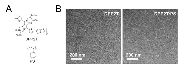
[Figure 2] (A) Molecular structure of DPP2T and PS. (B) Transmission electron micrographs of pure DPP2T thin films and DPP2T/PS thin films. It can be confirmed that a small amount of DPP2T is mixed with PS to form a network structure continuously connected to the DPP2T in a solution process that is different from pure DPP2T.
□ Professor Kwanghee Lee said, "The results of this research exceeded the possibilities of organic materials as electronic materials and implemented the functions that many have dreamed of. This new semiconductor technology, along with the transparency of ultra-thin films, which cannot be realized with existing silicon technology, provides a new paradigm to realize unique electronic devices, such as aesthetically superior wearable devices."
□ The results of this research have been carried out with the support of the Ministry of Science, ICT and Future Planning Basic Research Program (individual research), and it was published in the Proceedings of the National Academy of Sciences (PNAS) on November 22, 2016.