Media Center
A multimedia mosaic of moments at GIST
GIST Excellence
[Press Release] Professor Gun Young Jung"s research team develops inorganic-based transistor with foldable curvature radius of 1.5mm
- 엘리스 리
- REG_DATE : 2016.11.29
- HIT : 922
Professor Gun Young Jung"s research team develops
inorganic-based transistor with foldable curvature radius of 1.5mm

[Figure 2] Scanning electron microscope photograph after heat treatment. When PMMA is used as the gate dielectric material (left), it is observed that the IGZO thin film is cracked after heat treatment (bottom left). On the other hand, when SA7 is used as the gate dielectric material (right), the IGZO thin film does not crack after heat treatment. That is, the IGZO transistor based on the SA7 gate dielectric layer showed excellent heat resistance and durability without cracking on the semiconductor surface or the electrode even after the heat treatment.
□ Researchers at the Gwangju Institute of Science and Technology (GIST) have developed a mineral-based transistor that works even when bent over 1,000 times with a radius of curvature of less than 1.5 mm. This development will contribute to the commercialization of smart electronic devices that can be rolled or folded.
* Curvature radius: "curvature" refers to the degree of curvature, and the inverse number of curvature, "radius of curvature", means the radius of the curved line. The larger the curvature, that is, the greater the degree of curvature, the smaller the radius of curvature, and the smaller the degree of curvature, the greater the radius of curvature.
□ Existing flexible transistor materials widely use semiconducting polymer materials, but they are difficult to use in high performance electronic devices due to low electron mobility. The team succeeded in fabricating a flexible inorganic-based transistor consisting of an IGZO metal oxide channel with high electron mobility over a new polymer gate dielectric material. (See Figure 1)
* IGZO: An amorphous semiconductor material consisting of indium (In) - gallium (Ga) - zinc oxide (ZnO). It can be easily manufactured by solution process or simple sputtering, and has excellent electron mobility and light collection characteristics
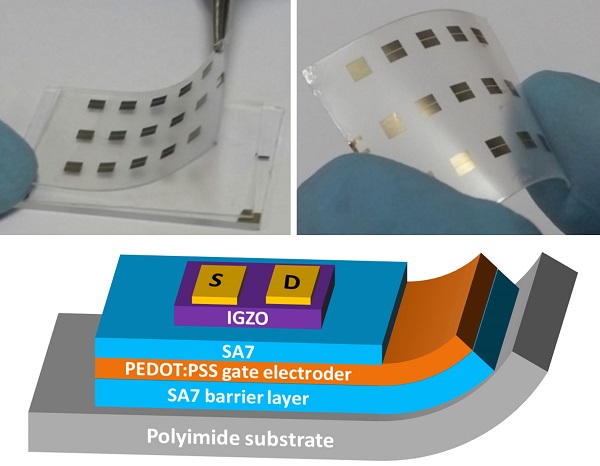
Figure 1 is a cross-sectional view of a polyimide-based flexible IGZO transistor. The IGZO-TFT fabricated on polyimide is weakly connected and can be easily separated from PDMS / glass substrate. IGZO-TFT can be manufactured because it can process spin-coating solution on flat PDMS / glass substrate and minimizes process defect between heat treatment by using polyimide substrate and SA7 gate dielectric material.
IGZO thin film deposited on PMMA, which is widely used as a gate dielectric material, can become cracked or wrinkled after heat treatment. However, the researchers used SA7, which has excellent thermal stability as a polymer gate dielectric material, and deposited thin films of IGZO without thermal cracks and wrinkles after heat treatment. (See Figure 2)
In particular, when bent at a radius curvature of 1.5 mm, the nano-wrinkles formed on the IGZO channel showed a resilience that disappears when the thin film is reopened. The IGZO thin film transistor (TFT) thus developed exhibited an electron mobility of 15.64 cm 2 / Vs, a threshold voltage of 6.4 V, and an on-off current ratio of 4.5 × 10 5.
* Threshold voltage: the minimum gate voltage that forms a channel through which charges in the semiconductor thin film can move when a certain potential difference is applied to the source-drain electrode of the transistor and a voltage is applied to the gate electrode. A high threshold voltage requires a small threshold voltage because power consumption increases during use.
On / off current ratio: The ratio of the saturation current to the base current during the operation of the transistor. The higher the ratio, the more effectively the amount of current flowing in the semiconductor can be controlled, resulting in a semiconductor with superior performance.
In addition, after enduring 1,000 or more bending tests at a radius curvature of 1.5 mm, the characteristics of the device hardly deteriorated. This corresponds to a bending strain of 3.33%, which is well above the maximum bending strain of 1.5% reported in the previously reported flexible IGZO transistor. (See Figure 4)
* Bending strain: a measure of the degree to which a material deforms when external bending stress is applied. The higher the bending strain, the greater the degree of deformation due to bending.

[Figure 3] (Left) When flexible IGZO transistor with a radius curvature of 1.5 mm are bent, IGZO channel nanocracks appear. (Right) When flattened after bending stress is removed, the nanocracks disappear and a very smooth IGZO channel can be seen.
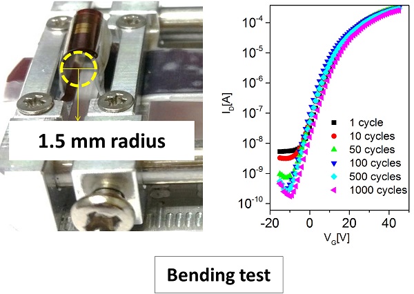
[Figure 4] Bending test with curvature radius of less than 1.5 mm (left) and graph showing transistor characteristics after 1,000 bending radius tests (right). After 1,000 bending tests, no degradation of transistor characteristics was observed.
□ Professor Gun Young Jung said, "The newly developed IGZO transistor has the potential to be applied to next-generation electronic devices that can be bent or folded. In the future, I plan to develop a flexible IGZO transistor that can be pulled like a rubber band and then returned to its original size. "
□ This research, led by Professor Jung and GIST Ph.D. student Yogeenth Kumaresan (India) and supported by the Pioneer Project of the Ministry of Science, ICT and Future Planning, the Korea Research Foundation, and the GIST Research Institute (GRI), was published on November 23, 2016, in Nature"s Scientific Reports.