Media Center
A multimedia mosaic of moments at GIST
GIST Excellence
[Press Release] Manufacturing ultra-thin metal-oxide films in 5 minutes
- 엘리스 리
- REG_DATE : 2015.05.26
- HIT : 833
Manufacturing ultra-thin metal-oxide films in 5 minutes
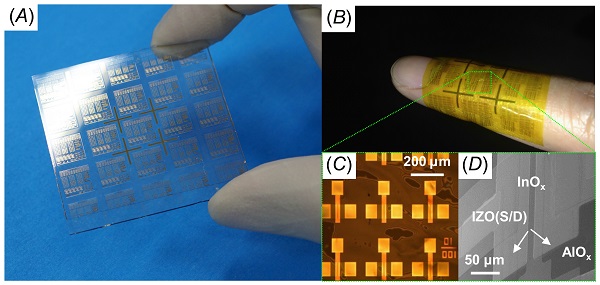
(Figure1) Manufactured metal-oxide and circuitry based on the all-solution process using deep ultraviolet in 5 minutes. (A) Metal-oxide device on top of a glass plate. (B) Flexible meal-oxide device on an ultra-flexible plastic that is as thin as a human hair. (C) and (D) are the close ups.
Korean researchers have developed a manufacturing process that only requires 5 minutes to complete which had previously required 2 hours. They were the world’s first to use the deep ultraviolet (DUV) via radical-mediated reactions to manufacture high-quality oxidation insulator.
The research was led by GIST Professor Myung-Han Yoon and Chung-Ang University Professor Sung-Kyu Park.

(left) GIST Prof. Myung-Han Yoon, Chung-Ang University Prof. Sung-Kyu Park, and GIST Ph.D. candidate Sung-Jun Park
Metal oxide materials have emerged as a promising platform because these materials demonstrated great potential for transparent electrodes, high-mobility semiconductors, and high-k dielectrics. Based on sol–gel chemistry, it is of particular interest because solid metal oxide materials with excellent electrical characteristics can be easily synthesized from small molecular precursors via simple solution processes, which herald a new era of very large-area electronics at an affordable cost.
The fabrication of sol–gel derived metal oxide electronic devices and circuits by low-temperature photochemical activation via in-situ radical-mediated reactions. The rapid photoactivation process enables the conversion of the sol–gel precursors into metal oxide electronic materials directly on ultra-flexible plastic substrates, which will serve as a general process for rapid and scalable commercial use.
* Radical: chemically reactive unpaired electrons that reacts quickly to chemical changes. (They have more than 2,000 times the ozone and 180 times of the sun’s ultraviolet ray’s oxidation rate.)
Oxide dielectrics typically require prolonged thermal annealing time at considerably higher temperatures than semiconductors to guarantee pinhole-free and densified films with minimal leakage current that have high capacitance values. Such time-consuming process requirements typically deter prompt preparation of sol–gel metal oxide dielectric films and scalable fabrication of all-solution-processed, high-performance metal oxide transistor arrays on unconventional substrates.
UV-based photochemical activation is dramatically more effective in terms of the subsequent film densification, polycondensation promotion, and impurity removal. The present thermally-assisted photochemical activation route will serve as a general method to enable the preparation of all solution large-area flexible displays and ultra-flexible wearable electronics in a rapid, scalable, and economical manner.
The paper has been selected to be the front cover story of the May 20th issues of Advanced Functional Materials.