Media Center
A multimedia mosaic of moments at GIST
GIST Excellence
Prof. Kwanghee Lee"s Team Develops Key Organic Electronic Material for Flexible Display
- 정명식
- REG_DATE : 2014.07.10
- HIT : 1624
□ A Korean research team has developed a key organic electronic material with a dramatically improved performance for the first time in the world. By developing a new technique that automatically aligns organic semiconductors, the researchers have enhanced charge transport of organic semiconductors by up to 100 times and replaced the conventional high temperature process with a new room temperature one. Their achievement is expected to greatly help improve the performance and accelerate the commercialization of organic electronic devices such as organic solar cells, flexible displays, and organic transistors. Figure 1: Mr. Sooncheol Kwon, Prof. Kwanghee Lee, and Dr. Heejoo Kim (from left to right)
The results were published in Nature Communications, a sister publication of Nature, as an online paper dated June 18, 2014 (Title: Template-mediated nano-crystallite networks in semiconducting polymers). The research was led by joint communicating authors Prof. Kwanghee Lee of GIST School of Materials Science and Engineering and Dr. Heejoo Kim of GIST Research Institute for Solar and Sustainable Energies, was conducted by first author Mr. Sooncheol Kwon, a Ph.D. student at GIST Department of Nanobio Materials and Electronics, and was supported by the NCRC (National Core Research Center) program of the NRF (National Research Foundation) and the MSIF (Ministry of Science, ICT, and Future Planning) and by the GIST Next Generation Solar Cell Technology Development program.
□ Unlike electronic devices based on inorganic materials, organic semiconductors can be coated on plastic substrates through a solution process, making them widely applicable to flexible displays and organic solar cells.
To fabricate high-performance electronic devices, the organic semiconductor molecules must be regularly arranged so that the charge carrier may travel easily. However, organic semiconductors by nature have irregular molecular arrangements, making them hard to be made into high-performance electronic devices. To overcome this problem, high temperature processes at 200°C or above have been tried, but they are difficult to be applied to plastic substrates and thus have limitations for flexible organic electronic devices.
□ The research team developed a new way of aligning organic semiconductor molecules based on the principle of static electricity. They mixed polymer templates having electrostatic characteristics with organic semiconductor solutions in order to induce strong electrostatic interaction between them. As a result, they succeeded in regularly aligning organic molecules along polymer templates and in increasing charge transport by at least 10 times and up to 100 times.
In addition, they succeeded in controlling organic molecules at a room temperature instead of a high temperature, ensuring applicability to organic solar cells, flexible displays, and various other organic electronic devices.
□ “These results have not only shown an innovative new method of aligning organic molecules but also enabled the fabrication of high-performance organic electronics at room temperatures; as such, they are expected to accelerate the commercialization of next generation organic electronic devices and wearable devices,” said Professor Kwanghee Lee.

Figure 2: Characterization of the template-mediated crystallization of P3HT
a) Ultraviolet–visible absorption spectra of the P3HT and P3HT:PSS solutions (dots) and films (solids). The inset presents the absorption spectra at 1,000 nm (1.3 eV), where a polaron transition occurs. (b) ESR spectra of the pristine P3HT, PSS and P3HT:PSS solutions. The g-factor is 1.9999. (c) X-ray photoemission spectroscopy (XPS) of the corresponding films. The slightly shifted binding energy of sulphur in the P3HT:PSS film (blue line) indicates the presence of positively charged sulphur. The inset reveals the presence of ionized PSS− in the P3HT:PSS film. (d) The sequential change of the nanomorphology of the P3HT:PSS film as a function of time (from 0 to 72 h) using high-angle annular dark-field scanning TEM (HAADF-STEM). Scale bars, 1 μm. (e,f) Electron dispersive spectroscopy on the selected region of the P3HT:PSS film after 24 h and the P3HT:PSS film after 72 h, respectively. Scale bars, 100 nm

Figure 3: GIWAXS investigations of P3HT and P3HT:PSS (1:1 w/w) films
(a,b) Two-dimensional GIWAXS from the pristine P3HT and P3HT:PSS (1:1 w/w) films on a silicon wafer. The incident angle was selected as 0.6°. (c,d) One-dimensional scattering profiles (out-of-plane and in-plane directions, respectively) obtained from the two-dimensional GIWAXS images. The insets show the incident direction of the X-ray beam.

Figure 4: Role of doping and template agents in π-CP films
(a) Schematic diagram of the categorization of doping and template agents depending on their chemical structure. The acidic molecules of MSA and TSS shown in the red panel and the non-acidic polymer of PSS−:Na+ and PS in the green panel are the doping agents and template agents, respectively; PSS is categorized in the intersection region and is called the bifunctional agent. (b) ESR spectra of the pristine P3HT, P3HT:TSS, P3HT:PSS and P3HT:PSS−:Na+ solutions. (c) Plot of charge-carrier density of the corresponding films measured in typical M-I-M configuration, ITO/semiconductor/aluminium. The inset presents a Mott–Schottky plot of the films. The error bars represent standard deviations derived from more than three devices. (d) Transfer characteristics of the corresponding PFETs on a Si++/SiO2 silicon wafer (tox~200 nm); the charge-carrier mobility of the P3HT:TSS film is on the order of ~0.01 cm2 V−1 s−1, whereas the mobility of P3HT:PSS−:Na+ is on the order of ~0.001 cm2 V−1 s−1. (e) High-resolution X-ray diffraction (HR-XRD) patterns of the corresponding films.
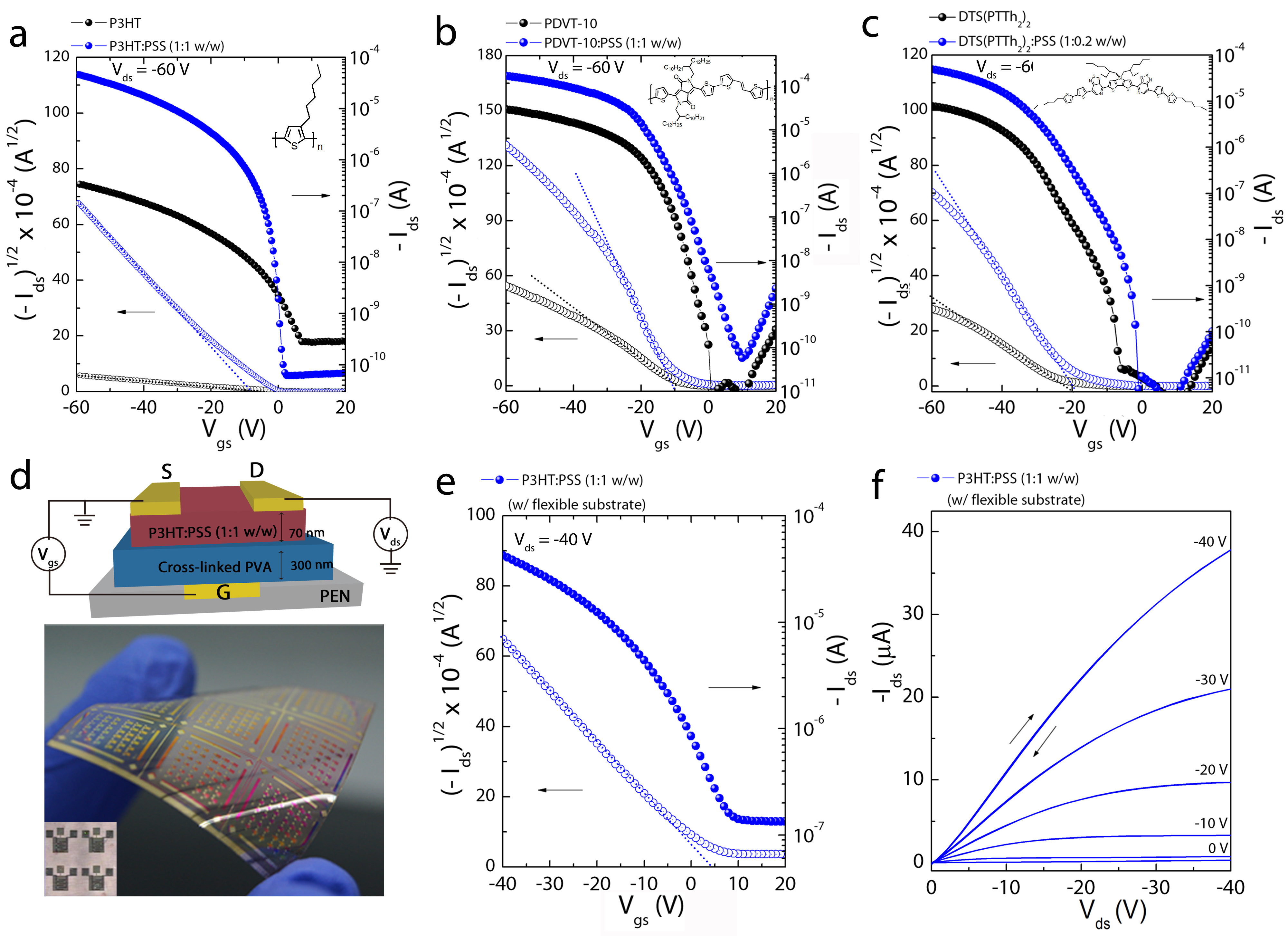
Figure 5: High-performance OFET devices with various π-CPs:PSS films
(a) Transfer characteristics of OFETs on a heavily n-doped Si/SiO2 silicon wafer (tox~200 nm) using P3HT semiconductors with and without the PSS template; the OFETs exhibit an improved charge-carrier mobility from 0.0009, cm2 V−1 s−1 to ~0.18 cm2 V−1 s−1. (b,c) Transfer characteristics of OFETs on Si++/SiO2 silicon wafers (tox~200 nm) using PDVT-10 and DTS(PTTh2)2 with and without the PSS template; the OFETs exhibit an improved charge-carrier mobility from 0.1 cm2 V−1 s−1 to 1.1 cm2 V−1 s−1 for PDVT-10 and from 0.03 cm2 V−1 s−1 to 0.27 cm2 V−1 s−1 for DTS(PTTh2)2, respectively. The insets show the respective chemical structures. (d) The schematic device structure and an image of the corresponding flexible PFETs with an area of 4.4 × 4.4 cm2 (324 devices). (e) Transfer characteristics of the flexible PFET devices with the P3HT:PSS film (1:1 w/w); the devices exhibit a saturation-regime mobility of ~0.25 cm2 V−1 s−1. (f) Output characteristics of the flexible PFET devices with the P3HT:PSS film (1:1 w/w).

Figure 6: Mechanism of the formation of TMC-induced fibril nanostructures
(a) Detailed mechanism of the electrostatic interaction between π-CPs (that is, P3HT) and the PSS template followed by hydrogen bonding, protonation and polaron formation in the solution state. (b) A schematic image of crystallized P3HT molecules along the PSS template via the electrostatic interaction between the P3HT and the template.